Warning: Constant automattic\jetpack\extensions\social_previews\FEATURE_NAME already defined in /home1/tessol/sbc-85.com/wp-content/plugins/jetpack/extensions/blocks/social-previews/social-previews.php on line 14

Warning: Undefined property: stdClass::$domain in /home1/tessol/sbc-85.com/wp-content/plugins/lava-bp-post/includes/class-core.php on line 355

Warning: Cannot modify header information - headers already sent by (output started at /home1/tessol/sbc-85.com/wp-content/plugins/jetpack/extensions/blocks/social-previews/social-previews.php:14) in /home1/tessol/sbc-85.com/wp-includes/feed-rss2.php on line 8
SBC-85 http://sbc-85.com New Homes for Vintage Chips Mon, 11 Jul 2022 01:49:15 +0000 en-US hourly 1 https://wordpress.org/?v=6.5.3 http://sbc-85.com/wp-content/uploads/2020/01/cropped-IMG_9077-scaled-1-32x32.jpg SBC-85 http://sbc-85.com 32 32 205200050 SDK-85? Does Anyone Want a New 8755 Project? http://sbc-85.com/does-anyone-want-a-new-8755-project/ Sun, 10 Jul 2022 19:13:21 +0000 http://sbc-85.com/?p=41496

The first single board computer that I wire wrapped was the Intel 3-chip MCS-85 minimum system with an 8085 CPU, a 8156 RAM + I/O, and a 8755 EPROM and I/O.  The second that I wire-wrapped was a SDK-85 that I thought would be a great Christmas present for [who is now] the Mrs.  (As it turns out, she wasn’t as excited about the SDK085 as I was).

My homemade SDK-85 not only taught me the 8085, but it taught me a lot about selecting presents for the Mrs.

I had a great fondness for those boards. so sometime later i turned these little wire-wrap creations into real circuit boards, but sometime over the last 40 or so years these have all [mysteriously] gone missing and I have given up on ever finding my beloved original wire wrapped boards or their PCB versions.

I have thought about bring them back and sharing the project, but these rely on the 8755 EPROM and, as you may know, not every grandmother has an 8755 programmer.  My Needham EMP-20 remains my workhorse for the 8755 (and MCS-48 projects) but not everyone is so fortunate to have one of these.   I had started recreating these boards as (yet another) back burner project, but because these boards require the 8755 and most can’t program that chip, I wasn’t considering adding them to the SBC-85 family of shared projects.

However, recently I came across Matt Millman’s project page for his MCS-85 Arduino shield and adapter board for the 8755 which is making me reconsider finishing these out as SBC-85.COM projects.

As I remember the minimum system board, my version had the 8085, 8156, and 8755, but it also had a socket for the Intel 8185 1KB RAM.  

My original wire-wrapped was a single board, but the PCB version of my SDK-85+ was a two board system, one was the keyboard and display and the other the main board.  Like the original Intel SDK-85, my main board had an 8085, a pair of 8155s, and a pair of 8755s so it could run the original Intel SDK-85 resident monitor.  But I also added a couple of EPROM sockets and sockets for one or two 8185 RAMs if i could ever afford them (I don’t remember if the 8185s were ever populated actually).

Updated SDK85+ Core SBC board with 8085, 2x 8155, 2x 8755, 2x8185, 2 EPROM sockets, 72 bits of I/O

I used a much improved resident monitor on my SDK85 that used a terminal for disassembly, changing registers, etc., so the keyboard / display wasn’t required like the original SDK.  Nonetheless, the displays and keypad were great for program input and display.  An especially fun project that I remember, was learning to program programming the 8279 keyboard / display controller to create a musical piano / organ keyboard.   Is it any wonder why we reminisce about those days of simple challenges and simple accomplishments?

Since I needed to start the boards from scratch, I have decided to update some components and change the EPROMs to universal sockets and add a MAX232 so I could drop the +/- 12V power supply.  I also added a few more keys to the keypad and a few more digits to the display.  If you prefer, you can break the display at the tab and put on little hinges to make it easier to view or panel mount.  Other than that, as best as I can remember them, I think that I have pretty much stuck to my original design.

The keypad / display board has the 8279 keyboard / display controller and three Vishay TDC 0.39″ Quad Display Modules for a total of 12 digits.

the main CPU board and the (optional) keypad / display board use a short IDC ribbon cable, but you could put in straight M/F headers and directly plug the boards together I suppose.

Updated SDK-85+ two board set. 8279, 29 Cherry MX keys, 12 digit 7-segment display,

These are still a back burner project for me and I don’t know when they will get finished and off to the PCB house.  But if you miss having the 8755 on your bench, maybe these would be projects of interest to you?  Let me know!

]]>
41496
STD Bus Prototyping Board http://sbc-85.com/std-bus-prototyping-board/ Sun, 29 May 2022 20:41:46 +0000 http://sbc-85.com/?p=41428

I needed a STD bus pad-per-hole prototyping card and it seems useful enough to take the trouble to document and share with others.

This card is STD Bus standard size and provides a nice pad-per-hole prototyping area with power and ground rails.  As with my other prototyping cards the +5V pads are square and the 0V pads are oval.  The signal names are nicely labeled front and back, a few test points for power rails, and so forth.  The documentation and build files are available here.

Since this is a first version of the board, please let me know if you find any mistakes. Thanks!

]]>
41428
The Fairchild F8 Single Board Computer Gets me Out of My Wheelhouse http://sbc-85.com/the-fairchild-f8-gets-me-out-of-my-wheelhouse/ Sat, 21 May 2022 01:17:20 +0000 http://sbc-85.com/?p=41362

A few months ago, my new buddy Will sent a couple of Mostek MK38P70 microcontrollers and suggested I could make something useful out of them.  Being intel brainwashed at a tender age, I knew next to nothing about the F8 and absolutely nothing about Mostek’s second generation F8, the 3870. However, considering the F8 was the most popular microprocessor in 1977 and the 3870 was the first microcontroller, i was quickly onboard with yet another new project.

A first version of the F8 Single Board Computer (SBC) was been completed and tested, and it was now time to buckle down and figure out why the F8 had such a terrible reputation of being a quirky microprocessor.  Fairchild’s “Guide to F8 Programming” has been my bedside companion for a month now, I have assembled hundreds of lines of code, have tested all aspects of the little board, have beaten it into submission, and finally consider myself to be an amateur F8 programmer.

It is time to welcome others to the project by making the build files and documentation available for download.  Eventually I will get around to making another version of the board, but in the mean time this version is an excellent development / training platform.  Check out the youtube playlist, the schematic and User’s Manual and let me know what features you think should be added to the next revision.

While they last, i have these listed on tindie if you would like one.  Eventually this will be replaced with the next revision of the board.

]]>
41362
STD Version of the SBC-85 CPU Board is in the works http://sbc-85.com/std-version-of-the-sbc-85-cpu-board-is-in-the-works/ Wed, 23 Feb 2022 23:24:39 +0000 http://sbc-85.com/?p=40817

 I have decided to port the SBC-85 8085 CPU board over to STD Bus.    I am just at the design stage so if you want to have any input, now is the time.

One of the biggest features that people have been asking for the SBC-85 is to create a CP/M version which has RAM starting at 0000h and boots to upper ROM.  While that is going to be a tough feature to add in the 100mm x 100mm format of the SBC-85, I may try again after I get this board completed. 

If you are interested in this STD Bus version of the SBC-85, send me an email on the contact us page and i will email you the current version of the schematic.  I don’t plan on posting it to this site until it is done because it would be just be one more thing that needs to be updated.

So this board is going to be the 6.5″ x 4.5″ to match the STD requirements and it should have all the handshaking lines to meet the STD Bus specifications and to allow DMA, etc.  Like the SBC-85 CPU board, it will have a RS232 port hanging on the SID and SOD lines, it will have the 8155, two EPROMs, and a 6264 RAM.  I am also aiming to have a little pad-per-hole sandbox so everyone can do a little bit of tinkering with add-ons.

There will be lots of testpoints around on key signals so you can drop in a patch wire or a wirewrap pin and grab signals, unused gates, interrupts, etc., and take them to the sandbox or the I/O connector for offboard use.  Speaking of the I/O header, it has been increased to a 34 pin header which gives us all the 8155 signals and the original 2X power and 2X ground lines, but now there are an additional eight unused lines that can be patched to other signals to take to the offboard protoboard.  Yes, that means this version of the header will not be compatible with the existing version of the protoboard but sometimes progress is painful.

Let me know if you have any input, since i am a bare metal man, I am especially interested to hear from CP/M gurus that can give me feedback on my memory swapping plans.

Documentation for this STD Bus 8085 SBC is here

-Craig

]]>
40817
Guus Assmann’s SBC-Z80 added to the SBC-85 Ecosystem http://sbc-85.com/guus-assmanns-sbc-z80-added-to-the-sbc-85-ecosystem/ Sat, 10 Jul 2021 23:10:15 +0000 http://sbc-85.com/?p=40794 In my last post I introduced Guus Assmann’s SBC-V20 board, here is his SBC-Z80 version whose design files can be downloaded here.

Guus’ SBC-Z80 is built upon the just4fun @hackaday project 159973 Z80-MBC2: a 4 ICs homebrew Z80 computer applied to the SBC-85 backplane. Like the SBC-V20 project, an Atmel Mega32A microcontroller is the system workhorse providing ROM and I/O which includes an I2C port that communicates with a Microchip MCP23017 port expander.

Guus Assmann’s Mega32A SBC-Z80 Single board Computer

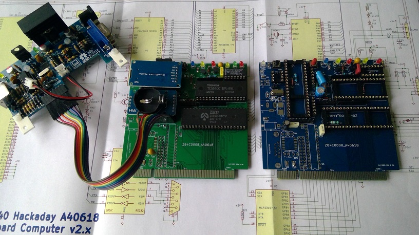
The SBC-Z80 begins with the original SBC-85 backplane pinout and has further claimed a handful of previously unused pins HALT*, WAIT*, RFSH*, INT*, IORQ*, BUSACK*, and BUSRQ*). Like the original SBC-85 CPU board, the SBC-Z80 has a DB9 serial port with a MAX232 to generate true RS232 signal levels but it also brings off board the raw Mega32A signal levels for use with one of those handy TTL/CMOS to USB serial port adapters. Two of Guus’ completed boards are shown in the photograph, the one on the left has a micro SD and real time clock (via I2C) installed and a cable to a terminal board.
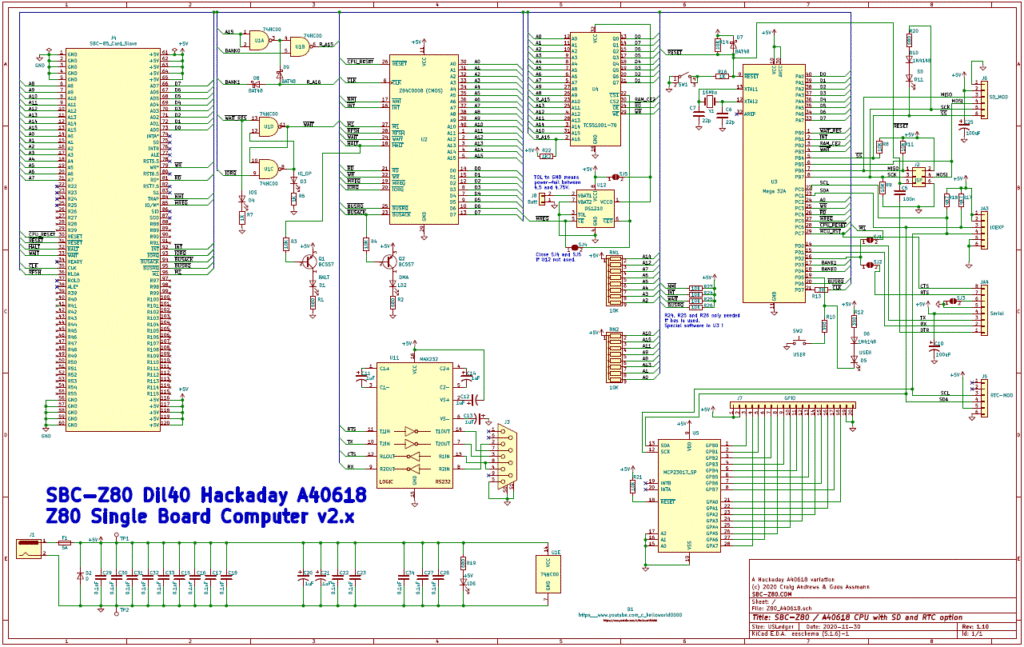
Guus Assmann’s Mega32A SBC-Z80 Single Board computer Schematic

Primary components:

  • Z80 CMOS CPU
  • Atmel Mega 32A MCU
  • 551001 (128KB) w/ DS1210 RAM controller
  • MCP23017 port expander (I2C)
  • MAX232 TTL / RS232 Level Shifter

I/O:

  • SD Module with virtual disk capability
  • Real Time clock Module
  • 2x 8-bit I/O Expansion
  • 115K RS232 Serial Port (with CMOS level header)
  • ISP for programming the Mega32A
  • 120 pin backplane (à la SBC-85)

Guus’s project package including the assembly manual, BOM, schematic, and KiCAD source files, and Gerber build files are available here (link). Software and more description is on Hackaday under the base design by just4fun @hackaday project Z80-MBC2: a 4 ICs homebrew Z80 computer (link). I will leave it up to Guus to let us know how compatible the SBC-V20 and SBC-Z80 boards are with the other SBC-85 expansion cards. For questions regarding Guus’ SBC-V20, leave a comment for Guus or send me an email on my contact page and I will forward it to him so you can communicate directly.

]]>
40794
V20 Single Board Computer Added to the SBC Ranks http://sbc-85.com/v20-single-board-computer-added-to-the-sbc-ranks/ Fri, 09 Jul 2021 23:31:53 +0000 http://sbc-85.com/?p=40763 For those SBC-85 advocates that have been longing for the power and prestige that comes with the Z80 or 8086, Guus Assmann has been one of The Netherlands’ busiest beavers this last year contributing to the SBC-85 ecosystem. Last year while Covid was in full swing, I swapped a few emails with Guus regarding the SBC-85 platform and gave him my blessing and encouragement to create a Z80 version. I then continued with my Covid long-haul recovery, survived the 2020 US presidential election and subsequent brouhaha, got vaccinated when my number finally came up, and finally moved back into my summer hobby. That pretty well sums up my last 18 months — and yet I am still unable to completely comprehend (and probably unprepared for) the discontinuity that will forever exist between 2019 and 2022.

Over the last year I received the occasional ping from Guus providing updates on his progress, but had not actually sat down to look over his accomplishments until now and, to say the least, I am incredibly impressed. This prolific engineer has created both V20 and Z80 single board computers based on the SBC-85 backplane as well as almost a dozen other boards, resident monitors, and support software. Fortunately for all of us, Guus has been gracious enough to share his design files for inclusion on the SBC-85.com site.

Guus’ SBC-V20 is built upon the just4fun @hackaday project V20-MBC: a V20 (8088 + 8080) CPU homebrew computer A170924 (link) as applied to the SBC-85 backplane. An Atmel Mega32A microcontroller is the system workhorse providing ROM and I/O which includes an I2C port that communicates with a Microchip MCP23017 port expander.

Guus Assmann’s SBC-V20 Single board Computer

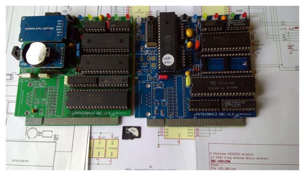
The SBC-V20 begins with the original SBC-85 backplane pinout and has further claimed a handful of previously unused pins (HLDA, HOLD, INTR, SSO*, DT/R1*, NMI, and S0*). Like the original SBC-85 CPU board, the SBC-V20 has a DB9 serial port with a MAX232 to generate true RS232 signal levels but it also brings off board the raw Mega32A signal levels for use with one of those handy TTL/CMOS to USB serial port adapters. Two of Guus’ completed boards are shown in the photograph, the one on the left has a micro SD and real time clock (via I2C) installed along with 1MB RAM, while the one on the right shows the board without the add-on modules and 128KB of RAM.
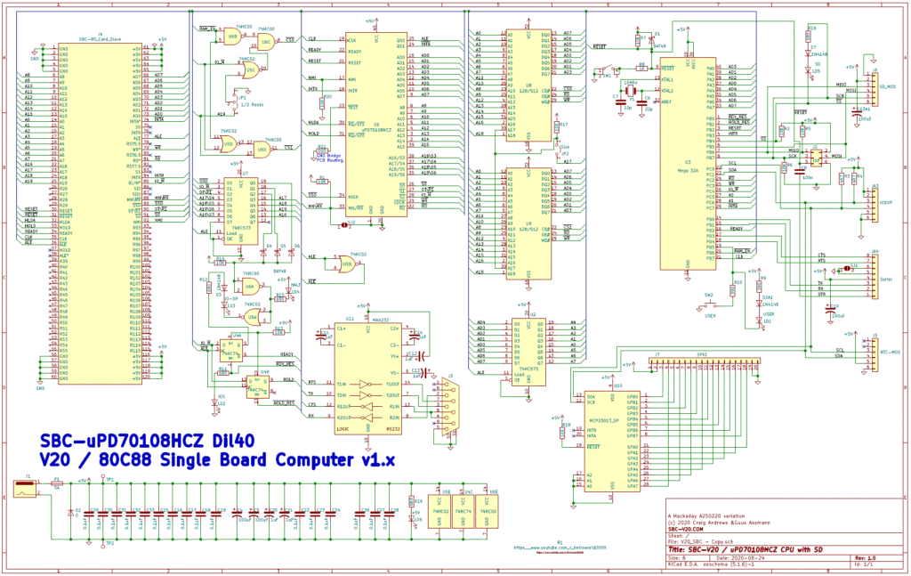
Guus Assmann’s SBC-V20 Single Board computer Schematic

Primary components:

  • uPD70108 CPU
  • Atmel Mega 32A MCU
  • 55100 (128KB) or 624006 (512KB) RAM
  • MCP23017 port expander (I2C)
  • MAX232 TTL / RS232 Level Shifter

I/O:

  • SD Module with virtual disk capability
  • Real Time clock Module
  • 2x 8-bit I/O Expansion
  • 115K RS232 Serial Port (with CMOS level header)
  • ISP for programming the Mega32A
  • 120 pin backplane (à la SBC-85)

Guus’s project package including the assembly manual, BOM, schematic, and KiCAD source files, and Gerber build files are available here (link). Software and more description is on Hackaday under the base design by just4fun @hackaday project A170924 (link) I will leave it up to Guus to let us know how compatible the SBC-V20 and SBC-Z80 boards are with the other SBC-85 expansion cards. For questions regarding Guus’ SBC-V20, leave a comment for Guus or send me an email on my contact page and I will forward it to him so you can communicate directly.

]]>
40763
SBC-85 CPU v2 COM Mistake http://sbc-85.com/sbc-85-cpu-v2-com-mistake/ Fri, 11 Sep 2020 23:06:13 +0000 http://sbc-85.com/?p=40671

Charles in Tennessee was having trouble with his USB to RS232 adapters working with his version 2 SBC-85 CPU board. It was working fine with the native COM port on his computer, but refused to communicate reliably when using a USB adapter. I have used the same board many times on both without issue, so I was afraid did not have any good suggestions other than my experience with USBs occasionally locking up and needing reset.

Fortunately, Charles completely ignored me and dug and dug until he found the problem was in the SBC-85 board, and not the adapter. He reported back to me today his findings and it was a real forehead-slapping moment for me.

As a bit of background, the first version of the SBC-85 CPU was created using Target 3001!. The goal of version 2 was to have universal EPROM sites which required a much tighter layout and KiCAD has features to make that easier, so the schematic and entire PCB layout was recreated using KiCAD. Long story short, I missed the ground on the DB9 for the COM port on the SBC-85.

A quick check of the schematics (below) show it was there on the version 1 board but missing on v2. The shield of the connector is grounded, but not the actual common (pin 5) of the connector.

Unfortunately, I also made this mistake on the SPIO board.  No excuse for that one.


Fortunately an easy fix, so take pin 5 over to one of the shield connections which are tied to the ground plane.

]]>
40671
SPIO v1.0 Under Test and Available http://sbc-85.com/spio-v1-0-under-test-and-available/ Fri, 24 Jul 2020 01:30:05 +0000 http://sbc-85.com/?p=40644

Version 1.0 of the Serial, Parallel I/O board features RS232 up to 19.2K, 24 pins of I/O on the 8255 PPI, 8 bits of home-brew output or input, and a predecoded expansion bus for off-board playground.  The documentation is in progress and draft versions have been uploaded.  So far there are a couple of mistakes, e.g., PC6 and PC7 are transposed on the J5 header.

]]>
40644
An Updated SPIO Board is Off to the Fab House, Hopefully it isn’t as goobered up as the prototype. http://sbc-85.com/an-updated-spio-board-is-off-to-the-fab-house-hopefully-it-isnt-as-goobered-up-as-the-first-version/ Sun, 12 Jul 2020 23:55:13 +0000 http://sbc-85.com/?p=40616

Well, I really pulled a boner by not reading the RTC specification sheet for the SPIO board and it came back to bite me.

Since I was going to submit boards in a couple of days, I did a quick design and layout of the Serial – parallel I/O board and slapped on a RTC with just a quick glance of the spec sheet. I could not see how they were decoding the internal ports but this was no time for learning or wading through pages and pages of blah blah blah. My plan was to figure that out when I sat down to start programming the RTC.

Well, the good news is that the 8251 USART works (thanks to Jack who caught a mistake in the baud rate clock), the 8255 works, and the onboard home brew I/O port works.

The bad news is that not reading how the spec sheet made the RTC a total failure. When I first looked at the specs it seemed too ridiculous to imagine that the chip actually took 128 I/O port addresses. I figured that there must be some sort of internal pointer that was loaded to  determine which of the internal ports was being accessed but, nope, the chip actually takes half of the available 8085 port addresses.

Yes, I could have either memory mapped the I/O (so the registers could have just been read as memory addresses), or I could have put in a ‘pointer’ port that would be loaded to then determine which port is actually being addressed. However, either of these would require a complete re-layout of the board and I was a little too disgusted at the RTC design to put any more effort into the parallel RTC.  I2C RTCs are readily available and just as useful, so I just bagged the RTC portion and replaced it with an expansion port header.

This header can be used with the Port Protoboard for off-board prototyping. The port address is already decoded and all the unused gates are brought to the prototyping header. In the end, even while the RTC was a disaster, the board should be a handy tool for experimentation.

]]>
40616
Serial – Parallel – I2C (SPI2C) v0.9 Prototype Going to Fab http://sbc-85.com/spi2c-v0-9-prototype-going-to-fab/ Sun, 12 Jul 2020 23:00:38 +0000 http://sbc-85.com/?p=40602

An easy derivative of the SPIO (Serial, Parallel I/O) board is a version that has an I2C controller in place of the I/O port expansion header.   So introducing the Serial, Parallel, I2C (SPI2C) SBC-85 board.  This is a 2-layer, 100mm x 100mm so fits in the super-cheap prototype special from the PCB houses.  The board offers an Intel 8251 USART for up to 19.2K Baud RS232, an 8255 24-pin parallel I/O port, and the I2C controller.

The Philips PCF8584 I2C controller (spec sheet) requires two I/O ports so I removed the expansion port header and onboard home brew I/O port to free up two I/O addresses. This also left a little room for a 10×10 pad per hole sandbox playground to populate your favorite I2C chips like a RTC, temperature sensor, or whatever your heart desires. There is also a 4-pin header for off-board I2C projects like an I2C display, your Arduino, or who knows what you have laying around your bench that needs to be interfaced to the SBC-85 system.  Finally, a little interrupt patch area to let you wire-wrap your choice of which interrupt you would like to go where.

The PCF8584 is reasonably available for a few dollars so that should not be a show stopper and there are I2C devices for nearly any function you can imagine, so this should be a handy board to have as part of the SBC-85 ecosystem..

]]>
40602