When I was a University I remember using a Z80 STD bus board for some lab experiments. We had some wire wrap STD expansion boards to wire up some IO expansion stuff. It was a great introduction to embedded systems. We were using a C cross compiler hosted on a unix minicomputer and you push the compiled binary code to the boards with xmodem I think. I have recently been doing work on a Jetson Xavier so everything is hosted on the couple of hundred dollar development board.
If you have a spare CPU card that would be neat but if the postage to Australia is going to be a killer then don’t worry about it. I will keep an eye on your design an maybe pickup a board when you have completed it.
I created a new max232 because the one in KiCAD was 5 times larger than any other chip, but I have done that chip so many times I didn’t even check it for mistakes. Thanks for pointing that out!
As for the cross shorting of the switches, you are right, that was a bone head mistake and I like you4 idea of doubling the encoders and dropp8ng the multiplexer.
Good catches on both and the first to point out this glaring error.
What STD board would like?
]]>I like the memory switching but there looks like there could be an interaction between the main and swap blocks when larger than 8k blocks are mapped. e.g. I you had say a 8k EEROM and 32k RAM. If the initial mapping was 0x0000-0x1fff EEROM and 0x2000 – 0xa000 so SW2 1 closed and SW5 2,3,4,5 closed. Say you wanted swap map with RAM now at 0x0000-0x8000 so SW7 1,2,3,4 closed. With this switch configuration the switches will connect Q0B, Q1B, Q2B and Q0A lines together regardless of the bank selected and you have an address clash in both configurations. I am not sure if this is a valid configuration. You can avoid the conflict by never changing the size of a memory block only its function. It might be possible to put some diode isolation between the main and swap selection switches. Perhaps what you could do is duplicate U2 and only enable the 3 to 8 decoder depending if in swap mode or not. This might mean you can remove U5 so there is no chip count increase. This also removes one gate delay in the address decoding path. ]]>
The problem got fixed. In the zip file you find an other zip/rar file. This causes the above problem.
The solution is simple: BEFORE uploading the Gerber file to JLCPCB.com you remove this file (jlcpcb backplane production file.rar) or you ONLY upload this file (jlcpcb backplane production file.rar) to JLCPCP.com.
If you don’t do this you get the above error.
Kind regards,
Edzard
]]>Hi Edzard
Thanks for posting this info.
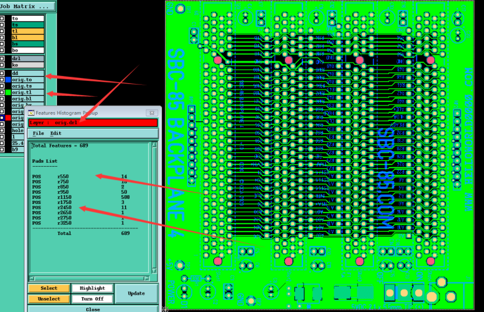
I (hopefully) have pasted the image you emailed below, perhaps someone can tell us what they are attempting to indicate as the error. It looks like there is a problem with the connector mounting holes since they are red, but i am not sure exactly what the problem is. Maybe because they are holes with zero (or near) pad thickness?
In the zip file there is a *.rar which is the file that JLCPCB sent back to me after they made the boards. So it *should* be ready to build since it is their file. The rest of the files in the ZIP are the original gerbers that i submitted to them. Just now i uploaded both of them to JLCPCB and both showed up OK in their gerber viewer. That is not always a perfect indication everything is OK, of course, but it is a start.
If you can get clarification on the error they are flagging that would be very helpful. You can also try removing their *.rar from the zip and resubmitting the gerber files themselves.
I looked back at the last time I ordered this board and there were some flags generated on another board submitted in the same order, but the backplane came back immediately approved for fabrication.
let me know if you find a work-around that solves the problem,
regards
craig
When ordering the latest Backplane version (V4) with JLCPCB.com I get the follwing remark from them:
” As shown below, is the file used for production before? if it’s production file, we will not make compensation for the files, is it OK? ”
Hmm, I can’t attach a file/picture here, I will w-mail it to you.
Kind regards,
Edzard
]]>I may not understand the question entirely, but maybe this will help….
The 8155 and others are agnostic about what instruction is used to access them, I.e., they just have an input pin that specifies if memory or I/O is being accessed and an enable pin. Not coincidentally, the 8085 has an output that is activated with the use of an IN or OUT command to indicate it is a memory or an I/O bus cycle. Since the data byte of the IN and OUT instruction can go from 00H to FFH there are 256 possible I/o ports that can be accessed using IN or OUT instructions. It is up to the hardware to decode which chip is being addressed during the memory or I/o cycle, I.e., by looking at the address lines and selecting or enabling a particular chip and also using the IO/M line to see if it is a memory or I/o. So while the 8085 can address 256 I/o ports, only the specific 8155 (or other I/o device) that occupies that address space should respond to the read or write instruction.
This is very related to your second question about how your old bingo machine works, if there are no IN or OUT instructions it likely is using memory mapped ports where I/o bus cycles are not distinguished from memory bus cycles, but rather the IO/M line is tied to an address bit. When using memory mapped I/o, the code can address a port using things like a STA LDA instructions or any other memory access instruction. This allows for much more convenient port access using a variety of commands AND provides for thousands of ports to be accessed.
Go back and look at your bingo code with an eye towards the memory access actually addressing I/o ports and you may be able to see what is going on. There is likely a block of memory with a certain address bit driving the 8155 IO/M line. When that line is high they are accessing an I/o port. When low, they are accessing memory.
Regards
Craig
]]>in the source file, change the definition of IBTIM and reassemble. that portion of the code is pasted below.
;********************************************************************
;************* SID / SOD SERIAL PORT MASKS, DELAYS ******************
;********************************************************************
;NORMAL SERIAL TIMER LOADS WHEN NOT USING DELAY SUBROUTINE
0033 IBTIM EQU 51 ;INPUT INTER-BIT TIME DELAY 2400 BAUD